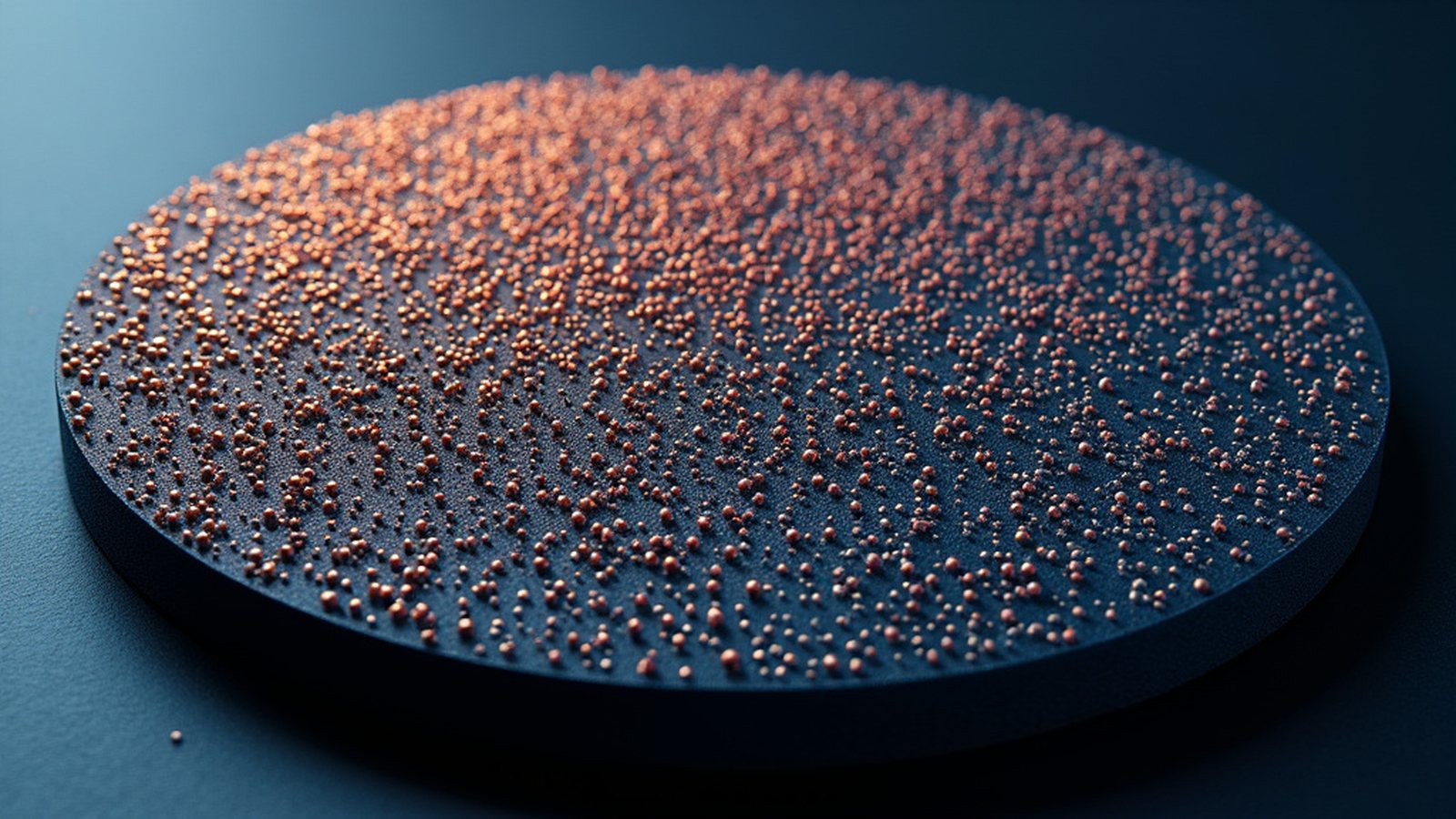
Researchers have developed a technique to produce environmentally stable p-type two-dimensional semiconductors at wafer scale by precisely controlling surface and near-surface atomic kinetics, according to a study published in Nature Materials. The finding offers a pathway for manufacturing scalable 2D complementary electronics.
Alessandro Molle and Yi Du reported that regulating atomic kinetics at and near the surface creates stable p-type two-dimensional (2D) semiconductor layers without degrading when exposed to ambient environments. Molle leads work at the Consiglio Nazionale delle Ricerche's Istituto di Microelettronica e Microsistemi in Agrate Brianza, Italy. Du conducts research at Beihang University's School of Physics in Beijing, China.
Wafer-scale electronics
The approach provides a foundation for scalable 2D complementary electronics, where stable p-type components are needed to pair with n-type materials for advanced computing circuits. Controlling surface dynamics enables uniform material growth across entire wafer substrates, addressing long-standing manufacturing challenges in 2D semiconductor fabrication.
Nature Materials published the peer-reviewed study on August 10, 2026. The paper cites foundational research on atomic kinetics and 2D systems, including 1997 findings in Science by Z. Zhang and M. G. Lagally, a 2011 Nature Nanotechnology paper by B. Radisavljevic and colleagues, a 2012 Advanced Materials paper by Y. H. Lee, a 2014 Nature Nanotechnology paper by L. Li, a 2018 Nature Electronics paper by Y. Wang, and a 2025 ACS Nano paper by Y. Tan. The publication also references 2026 studies in Nature Materials by S. Sun and Nature Electronics by L. Sun. Both authors declared no competing interests in the paper.